
The influence of arsenic layers on the electronic properties of GaN(0001) surfaces
We invite you to read a new work coauthored by dr Agata Sabik: Valence-band electronic structure of As-terminated GaN(0001) surfaces.
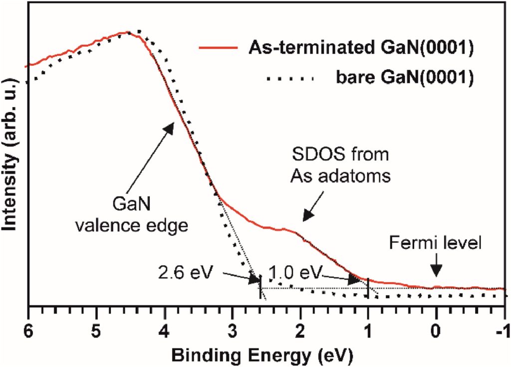
The work presents how arsenic layers influence the electronic properties of GaN(0001) surfaces. To learn about the key changes taking place in the electronic structure, the study employed photoelectron spectroscopy methods and calculations basing on the density functional theory (DFT).
To coat the surface with arsenic on the 0,25 monolayer (ML) level, each atom of arsenic merges with three atoms of gallium. Formation of Ga-As bonds effectively removes GaN surface states, which are the result of the presence of unsaturated chemical bonds. This action eliminates the pinning of the Fermi level near the edge of the conduction band and opens the way to control the electron properties.
At a coverage of 1 ML, new partially filled electron states appear in the GaN bandgap. Those additional states cause the valence band edge to be located closer to the Fermi level, which influences the application potential of this material.
The obtained results indicate that engineering GaN(0001) surfaces using arsenic atoms has a vast technological potential. This process can be applied in the production of advanced contacts on the basis of gallium nitride, which is crucial for the development of cutting-edge electronic and optoelectronic devices.
The figure presents the UPS spectrum of the valence band, obtained using a non-monochromatic photon flux with an energy of 21.2 eV, for As-terminated GaN(0001)-(1 × 1) (solid line) and pure GaN(0001)-(1 × 1) (dashed line).

